Beyond the Gigahertz Barrier: Engineering Signal Integrity Into High-Speed PCB Designs That Actually Perform

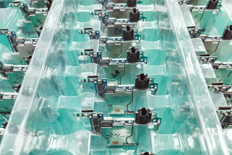
Photo: high speed PCB circuit board signal routing data center electronics engineering, via www.mokotechnology.com
When the Rules Change
There is a threshold in PCB design where the familiar assumptions stop holding. Below a few hundred megahertz, a trace is essentially a wire. Resistance and capacitance matter, but the electromagnetic behavior of the interconnect is largely forgiving. Push past 1GHz, and the physics asserts itself with increasing authority. At 10GHz and above, every millimeter of conductor, every via barrel, every reference plane gap becomes a potential source of signal degradation.
This is the domain that separates mid-range PCB designers from engineers working at the frontier of high-speed digital and RF design. It is also the domain that defines the performance envelope of modern 400G Ethernet switches, high-bandwidth memory interfaces, 5G base station hardware, and the dense compute platforms powering today's AI infrastructure.
Understanding what happens to a signal at these frequencies—and designing systematically to control it—is no longer a specialty skill reserved for a handful of microwave engineers. It is a core competency for any design team working on advanced communications or data processing hardware.
Impedance Control: The Foundation That Cannot Be Compromised
At high frequencies, a PCB trace is a transmission line. Its characteristic impedance is determined by its geometry—width, height above the reference plane, and the dielectric constant of the surrounding material—and must be controlled to within tight tolerances to prevent signal reflections.
For most digital high-speed interfaces, the target impedance is 50 ohms for single-ended signals and 100 ohms differential. Deviation from these targets generates reflections at impedance discontinuities that degrade eye diagrams, increase bit error rates, and in severe cases render a design non-functional regardless of how well the silicon performs.
Achieving consistent impedance requires a disciplined approach at multiple levels. First, the PCB fabricator must be selected and engaged as a technical partner, not just a manufacturing vendor. Controlled-impedance fabrication requires tight dielectric thickness tolerances, consistent copper plating, and precise trace etching. A fabricator who cannot provide impedance test coupons and measurement data on every panel is not an appropriate choice for 10GHz work.
Second, the stackup must be designed before layout begins—not after. The trace widths that achieve target impedance on a given layer are a function of that layer's distance to its reference plane and the dielectric properties of the material between them. Changing the stackup after routing begins can invalidate every controlled-impedance trace on the board.
Layer Stackup as a Signal Integrity Tool
The layer stackup is the most powerful signal integrity lever available to a PCB designer, and it is one of the most frequently underutilized. A well-designed stackup does several things simultaneously: it provides reference planes for every signal layer, minimizes the return current path for high-speed signals, separates power and ground planes to reduce simultaneous switching noise, and controls the dielectric properties that determine trace impedance.
For designs operating at 10GHz and above, a minimum of eight layers is typically required to achieve these goals without compromise. The canonical arrangement places signal layers adjacent to solid reference planes, with no two signal layers adjacent to each other without an intervening ground or power plane. This arrangement controls both impedance and crosstalk simultaneously.
Material selection becomes critical at these frequencies. Standard FR-4, the workhorse dielectric of the PCB industry, has a dielectric constant that varies significantly with frequency and a loss tangent that introduces unacceptable signal attenuation above a few gigahertz. High-speed designs at 10GHz and above require low-loss laminates such as Megtron 6, Rogers 4350B, or equivalent materials with stable Dk values and loss tangents below 0.005. These materials cost more and require process adjustments at the fabricator, but they are not optional at these frequencies—they are the price of admission.
Via Architecture: The Discontinuity You Cannot Ignore
Vias are among the most significant sources of signal integrity problems in high-speed PCB design, and they are also among the most frequently neglected. At low frequencies, a via is essentially invisible. At 10GHz, it is an impedance discontinuity with measurable inductance and capacitance that can degrade signal quality, introduce reflections, and create resonance artifacts.
The primary via challenge at high frequencies is the via stub—the unused portion of a through-hole via barrel that extends beyond the signal layer connection point. This stub acts as a resonant element whose electrical length becomes significant at high frequencies. A stub that resonates near the signal frequency can create a notch in the insertion loss curve deep enough to close the eye diagram entirely.
The solutions are well established but require intentional implementation. Back-drilling—mechanically removing the stub after board fabrication—is the most common approach for through-hole vias in high-volume production. For designs where back-drilling is not practical, blind and buried vias eliminate the stub problem entirely by connecting only the layers that require interconnection. High-density interconnect (HDI) stackups using laser-drilled microvias are increasingly standard in advanced high-speed designs for exactly this reason.
Antipad sizing also warrants careful attention. The antipad—the clearance cutout in reference planes around a via—disrupts the return current path and creates a local impedance discontinuity. Oversized antipads worsen the problem. Optimized antipad geometry, sometimes elliptical rather than circular for differential pairs, can meaningfully reduce via-induced signal degradation.
Crosstalk: Managing the Electromagnetic Neighborhood
At high frequencies, signals do not stay in their traces. Electromagnetic coupling between adjacent conductors transfers energy from an aggressor trace to a victim trace, introducing noise that degrades timing margins and increases bit error rates. This phenomenon—crosstalk—scales with frequency and becomes a dominant design concern above a few gigahertz.
Controlling crosstalk requires both spacing discipline and routing strategy. The 3W rule—maintaining a center-to-center spacing of at least three times the trace width between parallel high-speed signals—provides a practical starting point for reducing inductive and capacitive coupling. For the most sensitive signals, 5W or greater spacing may be necessary.
Parallel routing length is equally important. Crosstalk accumulates along the length of parallel runs, so minimizing the distance over which sensitive signals run parallel to each other reduces total coupling. Routing high-speed signals on orthogonal layers—horizontal on one layer, vertical on the adjacent layer—prevents long parallel runs even when routing density is high.
Differential signaling, now standard for most high-speed interfaces including PCIe, USB 3.x, and 100G+ Ethernet, provides inherent noise rejection when routed as tightly coupled pairs with matched lengths and consistent spacing. Breaking differential pair coupling—even briefly, to route around an obstacle—degrades common-mode rejection and should be avoided.
Simulation Before Fabrication
At 10GHz and above, the cost of a board spin driven by signal integrity failure is significant. Simulation using 3D electromagnetic tools such as Ansys HFSS, Cadence Clarity, or Keysight ADS is no longer a luxury for high-speed designs—it is a standard step in a responsible design process. Channel simulation using S-parameters from via and connector models, combined with time-domain analysis of eye diagrams under realistic jitter conditions, allows designers to identify and correct signal integrity problems before a single board is fabricated.
The investment in simulation pays for itself quickly. A single avoided board spin at advanced HDI tolerances typically covers the cost of the simulation tools and the engineering time to run them.
Engineering Signals That Survive Contact With Reality
High-speed PCB design at 10GHz and above is demanding precisely because the margin for approximation has disappeared. The physics is unforgiving. But it is also knowable, and the engineers who invest in understanding it—who treat impedance, via architecture, stackup design, and crosstalk as first-order design variables rather than afterthoughts—consistently produce hardware that performs as specified from the first build.
That is the standard the industry demands, and the standard that defines what it means to engineer tomorrow's circuits today.