Designing for a Frequency Future: The Hidden Cost of Locking Into 5G-Only PCB Architectures
For most American electronics manufacturers, 5G represents the current frontier. Commercial deployments are expanding, design tools have matured, and the component ecosystem has finally stabilized enough to support serious production commitments. It is, by most measures, an excellent time to design for 5G. The problem is that "excellent" and "future-proof" are rarely the same thing.
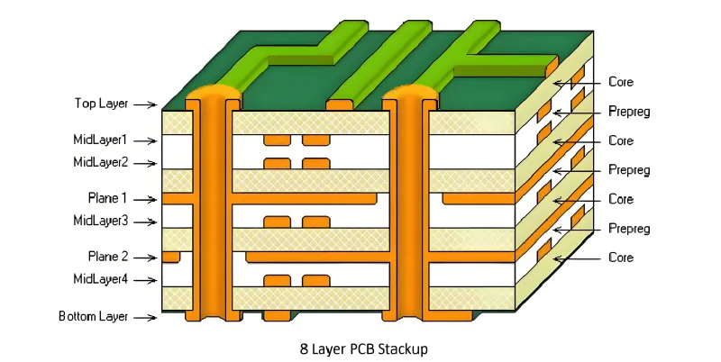
As 6G research programs accelerate at institutions like NYU Wireless, UC San Diego, and within DARPA-funded consortia, the sub-terahertz frequency bands being explored—ranging from 100 GHz to 1 THz—are not simply incremental extensions of existing 5G millimeter-wave architectures. They represent a fundamentally different set of engineering constraints. PCB designers who lock in material selections, layer stack-ups, and routing strategies optimized exclusively for today's 5G networks may find themselves facing expensive redesigns far sooner than anticipated.
What Changes at Sub-Terahertz Frequencies
At the frequencies where 5G millimeter-wave currently operates—typically between 24 GHz and 100 GHz—conventional PCB laminates such as Rogers 4350B or Isola I-Tera MT40 perform adequately. Dielectric loss is manageable, and transmission line geometries remain within the reach of standard fabrication tolerances.
Push into sub-terahertz territory and the physics become far less forgiving. Dielectric loss tangent values that are acceptable at 28 GHz become prohibitive at 300 GHz. Conductor roughness—a parameter that many designers treat as a fabrication nuisance rather than a performance variable—begins to dominate insertion loss. Surface roughness that measures 0.5 microns RMS may have negligible impact at 5G frequencies but can introduce significant attenuation at 6G bands.
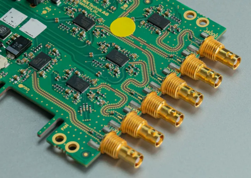
The antenna integration challenge also shifts dramatically. 5G antenna-in-package designs, while complex, have benefited from years of industry refinement. Sub-terahertz antennas require dimensional tolerances that push the boundaries of current PCB manufacturing capabilities in the United States. Beam steering arrays at these frequencies demand inter-element spacing measured in tens of microns—territory that currently belongs to semiconductor packaging, not traditional PCB fabrication.
The Real Cost of a Mid-Lifecycle Redesign
The engineering community tends to discuss obsolescence in abstract terms. The financial reality is considerably more concrete. A mid-lifecycle PCB redesign for a commercial wireless infrastructure product typically involves not only new layout and simulation work but also re-qualification of the entire assembly, updated regulatory filings, and potential disruption to customer supply agreements.
For defense and aerospace applications—where qualification timelines often stretch to 18 months or longer—the cost of a forced redesign due to frequency incompatibility can easily reach seven figures. Industrial IoT deployments, which are increasingly being specified with 10-to-15-year operational lifespans, face similar exposure. A gateway device designed and qualified in 2024 for 5G sub-6 GHz operation may require a complete board-level redesign to participate in whatever 6G ecosystem emerges by 2032.
The question is not whether 6G will arrive. The question is whether your current design will be capable of meeting it.
How Forward-Thinking Manufacturers Are Hedging
Some of the more strategically minded PCB design organizations in the United States are already adopting what might be called a "frequency hedge" approach. Rather than optimizing entirely for today's commercial specifications, they are making deliberate material and architectural choices that preserve upgrade pathways.
One common strategy involves specifying ultra-low-loss laminates—materials like Rogers 3003 or Taconic TLY—even for products that will initially operate at 5G frequencies. The cost premium is real but modest at the board level; the savings at redesign time can be substantial. The material selection does not guarantee 6G compatibility, but it avoids the most disqualifying limitation: a substrate with loss characteristics that cannot be improved through redesign alone.
Another approach involves modular RF front-end architectures. Rather than integrating the antenna array and the baseband processing onto a single rigid PCB, some designers are structuring the RF subsystem as a separable module with standardized interfaces. When frequency requirements shift, the module can be upgraded without disturbing the rest of the system. This adds design complexity and some cost at the outset, but it transforms a potential full-board redesign into a targeted module swap.
Simulation as a Strategic Tool
The electromagnetic simulation tools available to American PCB designers have become powerful enough to model performance across a broad frequency range during the initial design phase. Running full-wave simulations at both current 5G frequencies and projected 6G bands during the design review process costs time, not capital. It can reveal whether a proposed stack-up and routing geometry will degrade gracefully as frequency requirements evolve—or fail abruptly.
This kind of multi-frequency simulation discipline is not yet standard practice across the industry. Many design teams run simulations at the target frequency and consider the analysis complete. Extending that analysis to frequencies two or three times higher, even speculatively, provides a meaningful signal about architectural robustness.
The Procurement Dimension
Material availability is a practical constraint that cannot be ignored. Ultra-low-loss, high-frequency laminates are not stocked in the same quantities as standard FR-4 alternatives. American PCB fabricators who work primarily with commodity materials may not have the process experience to reliably fabricate with PTFE-based or ceramic-filled substrates. Designing for future frequency compatibility requires not only selecting the right materials on paper but also qualifying a supply chain capable of delivering them consistently.
This is where early engagement with fabrication partners matters. A PCB design that specifies Rogers 3003 but is destined for a fabricator with no experience processing it introduces manufacturing risk that can undermine the entire frequency-hedging strategy.
A Calculated Bet, Not a Guaranteed Win
It would be misleading to suggest that any design decision made today can fully accommodate 6G requirements that remain undefined. The 6G standardization process is years from completion, and the frequency bands that will ultimately be commercially deployed are still subject to regulatory and industry negotiation. What can be said with confidence is that designs built on the lowest-loss, highest-precision foundations available today will have more options when those standards arrive.
The frequency gamble is real. But it is not a binary choice between designing for 5G now and designing for 6G later. The most defensible position is to design for 5G today with materials, architectures, and simulation practices that preserve the maximum number of forward-looking options. That is not a hedge against failure—it is a commitment to engineering that outlasts the specification cycle that produced it.