Stack It Right: How Layer Architecture Shapes the Wireless Performance of Your Next PCB Design
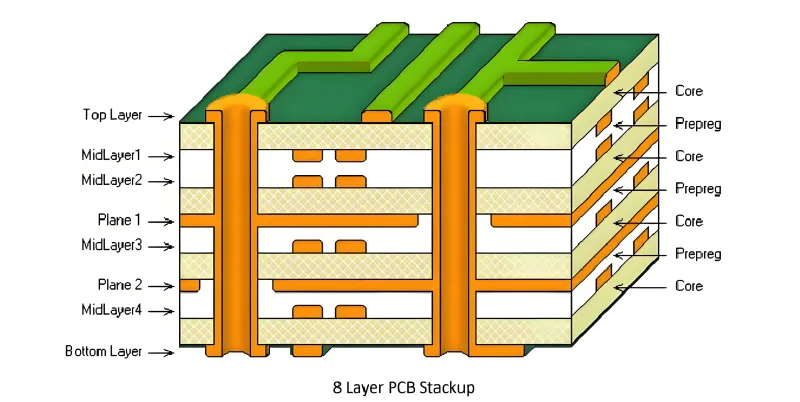
Photo: PCB multilayer stackup cross section RF wireless circuit board engineering, via jpfile1.oss-accelerate.aliyuncs.com
Wireless capability has become table stakes in modern electronics. From industrial sensors deployed across factory floors in Ohio to consumer wearables shipped out of fulfillment centers in Texas, the expectation that a device will connect reliably—at range, under interference, in real-world conditions—is now baked into nearly every product specification. What is less commonly understood is how profoundly the internal architecture of a printed circuit board shapes whether that expectation is ever met.
Layer stackup decisions are made early, often before the first schematic symbol is placed. They are also, paradoxically, among the most consequential choices a PCB design team makes for RF performance. Getting the stackup wrong does not always produce a board that fails to function. More often, it produces a board that functions poorly—one whose wireless range falls short of specification, whose signal quality degrades under thermal or mechanical stress, and whose behavior in certification testing becomes unpredictable.
Understanding why requires a close look at the physics that govern electromagnetic behavior inside a multilayer PCB.
Dielectric Material: The Medium Through Which Your Signal Travels
Every signal on a PCB travels through or adjacent to a dielectric material—the insulating substrate that separates copper layers. For low-frequency digital signals, the specific properties of that material matter relatively little. For RF signals operating at 2.4 GHz, 5 GHz, or millimeter-wave frequencies, they matter enormously.
The two dielectric properties that most directly affect RF performance are the dielectric constant (Dk) and the dissipation factor (Df). The dielectric constant determines the velocity at which signals propagate and influences the characteristic impedance of transmission lines. The dissipation factor quantifies how much signal energy is absorbed by the substrate as heat—a phenomenon known as dielectric loss.
Standard FR-4 laminate, the workhorse of the PCB industry and the default choice for the vast majority of commercial designs, has a Dk that varies with frequency and a Df that becomes increasingly problematic above roughly 1 GHz. For a product whose wireless radio operates at 2.4 GHz or higher, specifying FR-4 throughout the stackup is a choice that carries measurable signal attenuation penalties. Those penalties compound over transmission distance, which is precisely why a device that performs acceptably on the bench—where the wireless receiver is inches away—may underperform in the field, where the receiver is across a room or beyond a wall.
Low-loss laminates such as Rogers 4003C, Isola I-Tera MT40, or Megtron 6 offer substantially lower dissipation factors and tighter Dk tolerances. They also cost significantly more and introduce manufacturing complexity that can extend lead times and limit the pool of qualified fabricators. The engineering decision is not whether to use these materials universally, but rather where in the stackup they deliver disproportionate value.
Ground Plane Placement and the RF Return Path
Among the variables that stackup architecture controls, the positioning of ground planes relative to RF signal layers is one of the most impactful and least forgiving. A continuous, uninterrupted ground plane directly beneath an RF trace provides a controlled return current path, defines the transmission line geometry, and acts as a shield against electromagnetic interference emanating from adjacent circuitry.
When ground planes are fragmented—by routing slots, by thermal relief cutouts, or by traces that cross reference plane boundaries—return currents are forced to detour. Those detours create impedance discontinuities, generate unwanted radiation, and introduce the kind of unpredictable behavior that makes RF certification testing a costly ordeal. The further an RF signal layer is from its reference ground plane, the higher the impedance of the transmission line and the greater the susceptibility to coupling with neighboring signals.
In a four-layer stackup, the conventional layer ordering places signal layers on the outer surfaces with ground and power planes sandwiched between them. This arrangement provides reasonable RF performance for moderate-frequency applications. For designs operating above 5 GHz or requiring tightly controlled impedance across wide temperature ranges, a six- or eight-layer stackup may be necessary to position the RF layer within a few mils of a dedicated ground reference while keeping the power distribution network adequately decoupled.
Controlled Impedance: Precision That Starts at the Stackup
RF transmission lines—microstrip traces on outer layers, stripline traces buried between ground planes—must maintain precise characteristic impedance, typically 50 ohms for single-ended lines and 100 ohms differential for balanced structures. That impedance is a function of trace width, trace thickness, dielectric height, and dielectric constant. All of these variables are established, at least in part, by the stackup specification.
When a stackup is defined without reference to the impedance requirements of the RF signals it must carry, the result is a design that may require trace widths incompatible with the available routing space, or that can only achieve target impedance with dielectric thicknesses that introduce coupling problems between adjacent layers. The corrective iterations that follow—revising the stackup mid-project, renegotiating with the fabricator, adjusting trace geometry throughout the layout—are exactly the kind of schedule-consuming rework that erodes margins on competitive product programs.
The more disciplined approach is to begin stackup definition with the RF requirements on the table. Identify the target impedance values, the frequencies involved, the acceptable loss budget, and the routing density constraints before committing to a layer count or laminate selection. Work with the fabricator early—ideally before layout begins—to validate that the proposed stackup can be built to the tolerances the design demands.
Balancing Performance Against Production Reality
The temptation in RF-intensive designs is to specify the highest-performance materials and the most complex stackup the budget can accommodate. That instinct is understandable but not always correct. A twelve-layer board built entirely from low-loss laminate introduces fabrication complexity that can compromise yield, extend delivery timelines, and create supply chain dependencies that become liabilities when production scales.
The more practical approach is to use premium materials selectively. Hybrid stackups—combining low-loss laminate on the layers that carry RF signals with standard FR-4 on layers handling power and low-frequency digital signals—can deliver meaningful RF performance improvements at a fraction of the cost and complexity of an all-premium build. The key is identifying which layers genuinely require low-loss material and which are insulated from RF performance by their position in the stack.
This kind of targeted specification requires a clear understanding of the signal flow through the board and a willingness to engage with the fabricator as a technical partner rather than a commodity vendor. American PCB manufacturers with experience in RF and wireless applications can provide design-for-manufacturability guidance that prevents costly late-stage discoveries.
The Earliest Decision With the Longest Reach
Stackup architecture sits at the intersection of electrical performance, mechanical integrity, thermal management, and manufacturing economics. For products that depend on wireless connectivity, it also sits at the intersection of customer experience and competitive differentiation. A device that connects reliably at range, in challenging RF environments, and across the full operating temperature range delivers measurable value. A device that does not delivers returns, warranty claims, and negative reviews.
The engineering discipline required to define a stackup correctly—before layout begins, with RF requirements driving material selection and layer ordering—is not glamorous work. It rarely appears in product marketing materials. But it is precisely the kind of foundational decision that separates products that perform from products that merely function. For design teams building wireless-capable electronics in today's market, getting the stackup right is not optional. It is the starting point for everything that follows.