Passing the Lab, Failing the Field: The Impedance Mismatch Problem American Engineers Keep Missing
There is a particular frustration that seasoned PCB engineers know well: a board that passes every test on the bench, earns its certifications, ships in volume, and then begins generating field returns six months later. No obvious damage. No clear fault. Just degraded performance that no one anticipated because no one was looking for it in the right place.
Impedance mismatch is frequently the culprit — and the reason it escapes detection so reliably has as much to do with how American manufacturers structure their validation processes as it does with the physics of transmission lines.
Why Standard QC Protocols Miss the Problem
Most production quality control frameworks are built around pass/fail thresholds established during the design validation phase. Time-domain reflectometry (TDR) measurements confirm that controlled impedance traces hit their target values — typically 50 ohms for single-ended RF traces or 100 ohms differential — within an acceptable tolerance window. Those measurements are taken under stable, temperature-controlled laboratory conditions, using calibrated equipment and known signal sources.
The problem is that real-world operating environments are not laboratories. Temperature fluctuates. Connectors age. Board materials absorb humidity. And the cumulative effect of these variables on transmission line behavior is rarely captured in a standard production test plan.
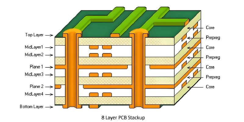
Consider a high-speed differential pair routed across a PCB stack-up that was designed and validated at 25°C. The dielectric constant of FR-4 — the most common PCB substrate in North American production — shifts measurably across a temperature range of -40°C to 85°C, a range well within the operating envelope of many commercial and industrial products. That shift alters the effective impedance of every transmission line on the board. In isolation, the change may be within tolerance. Compounded with connector impedance discontinuities, via stubs, and length mismatches, it can push a signal path well outside the design margin.
Standard QC does not test for this compound effect. It tests for each element in isolation, under conditions that favor passing.
The Case of the Wireless Gateway That Wasn't
One instructive example involves a mid-tier American electronics manufacturer producing industrial wireless gateway devices. The product passed RF compliance testing and signal integrity simulation with comfortable margins. Initial deployments performed exactly as specified.
Approximately eight months into the product's field life, return rates began climbing. Devices deployed in outdoor enclosures in the southeastern United States — where summer temperatures and humidity levels are both extreme — showed packet loss and intermittent disconnection that indoor-deployed units did not exhibit.
Post-failure analysis revealed a chain of compounding issues. The board's controlled impedance traces were manufactured at the high end of the tolerance window. The RF connector used for the antenna interface had an impedance characteristic that was technically within specification but consistently toward the low end. At room temperature, the mismatch was marginal. At elevated temperature, the substrate's dielectric constant shifted enough to widen that mismatch into a zone where reflected signal energy began causing measurable data errors.
The laboratory simulation had not modeled the connector's impedance characteristic at temperature. The production TDR sweep had not flagged the trace tolerance as a risk. The two issues existed in separate test silos, and the combination only became visible in the field.
Where the Design Process Breaks Down
This kind of failure reflects a structural limitation in how many organizations approach design validation. Simulation tools — even sophisticated 3D electromagnetic solvers — are only as accurate as the material models and boundary conditions that engineers provide. If those inputs are derived from datasheet nominal values rather than measured material behavior across operating conditions, the simulation is optimistic by design.
Connector and cable assembly impedance characteristics are frequently treated as fixed values when they are, in practice, distributions with temperature and aging dependencies. A connector rated at 50 ohms may perform at 48 ohms under one set of conditions and 53 ohms under another. When that variability interacts with trace tolerance and substrate variation, the combined impedance discontinuity can exceed what any individual specification would suggest.
The fix is not simply more testing — it is smarter testing. Worst-case analysis must account for the interaction of tolerances rather than treating each element in isolation. Thermal cycling should be incorporated into signal integrity validation, not treated as a separate environmental stress test.
Practical Steps for Closing the Gap
Several approaches have proven effective for American manufacturers seeking to align their validation processes with real-world performance expectations.
Stack-up material characterization across temperature. Rather than relying on datasheet values, engineers should request measured insertion loss and Dk data from their laminate suppliers across the full operating temperature range. This data, fed into simulation tools, produces substantially more accurate impedance predictions.
Connector characterization under load. RF and high-speed connectors should be modeled using measured S-parameter data rather than idealized specifications. Many connector manufacturers provide this data on request; when they do not, independent characterization is worth the investment for volume production designs.
Combined tolerance analysis. Impedance budgets should be calculated using worst-case combinations of trace tolerance, material variation, and connector impedance distribution — not nominal values alone. A design that passes with 10% margin at nominal may have no margin at all when tolerances stack unfavorably.
Environmental stress testing with signal monitoring. Thermal cycling and humidity exposure testing should include real-time signal integrity monitoring, not just post-stress electrical testing. Failures that appear only under active thermal stress may recover before a post-stress measurement is taken.
A Competitive Imperative
For American PCB manufacturers competing against lower-cost offshore alternatives, field reliability is one of the most defensible competitive advantages available. A board that passes the lab but fails the field does not just generate warranty costs — it damages customer relationships and opens the door to competitors who can demonstrate superior long-term performance.
Closing the impedance mismatch blindspot requires investment in more rigorous validation methodology, but the return on that investment is measured in reduced field failures, stronger customer retention, and a reputation for engineering quality that price alone cannot replicate. The physics of transmission lines are unforgiving. The validation process must be equally rigorous.