Passing Every Check, Failing the Factory: The Verification Gap That PCB Design Software Can't Bridge

Photo: PCB design engineer reviewing circuit board layout on computer screen in electronics lab, via bigshop.mk
There is a particular frustration familiar to experienced PCB engineers: a design that clears every automated rule check, satisfies every constraint manager flag, and generates a clean Gerber output—only to return from the fabricator with a list of manufacturability concerns that no tool ever flagged. The board passed. The factory said no.
This scenario is not rare. It is, in fact, one of the more persistent and costly inefficiencies in modern electronics development. As design software has grown increasingly sophisticated, a false confidence has taken root in some engineering teams—the belief that a clean DRC output is equivalent to a manufacturable design. It is not. The verification gap between what software validates and what a fabricator actually requires remains substantial, and understanding its contours is essential for any team serious about bringing boards to production reliably.
What Design Software Is Actually Checking
PCB design tools perform an enormous amount of useful work. They enforce clearance rules, flag unconnected nets, verify impedance targets against theoretical stackup models, and check pad geometries against component land patterns. For the purposes of schematic integrity and basic electrical correctness, modern EDA platforms are genuinely powerful.
The critical word, however, is theoretical. Design tools operate on idealized models. When a constraint manager evaluates a controlled-impedance trace, it is calculating against a stackup that exists as a set of numbers in a configuration file—not against the actual dielectric material that a specific fabricator sources from a specific supplier, processed through a specific lamination press on a given day. The tool does not know what your fabricator's copper foil roughness specification looks like. It does not know how that shop's etching chemistry behaves at the line widths you have specified. It does not know whether the via drill tolerances in its default library match the capabilities of the drill equipment on your fabricator's floor.
The software is checking your design against its own internal rules. Your fabricator is checking your design against reality.
The Stackup Assumption Problem
Layer stackup is one of the most consequential areas where this gap manifests. Engineers frequently build stackup definitions within their EDA tool using generic dielectric constants and copper weights that approximate industry norms without reflecting any specific fabricator's actual material set.
When that design reaches a shop, the fabricator constructs the board using the materials they stock and the processes they run. If the designed stackup calls for a 0.1mm dielectric with an Er of 3.9 but the fabricator's standard build uses a slightly different prepreg combination that yields an Er of 4.2, the impedance of every controlled trace on that board shifts. Whether that shift matters depends on the application—but in high-speed digital or RF designs, it can mean the difference between a functioning product and an expensive pile of scrap.
The solution is not simply to demand tighter material specifications. It is to engage fabricators early, obtain their actual stackup documentation, and build your design against their real process—not against a generic approximation. This requires treating the fabricator as a design partner rather than a downstream vendor, a shift in workflow that many US development teams have been slow to embrace.
Tolerances That Tools Don't Model
Beyond stackup, there is an entire category of manufacturing tolerances that EDA tools handle poorly or not at all. Drill registration tolerances, copper etching bias, solder mask expansion, and via-to-pad annular ring variation are all process-dependent parameters that vary between fabricators and even between process runs at the same facility.
A design tool may flag an annular ring as technically compliant against a generic IPC minimum. But if the fabricator's drill registration tolerance is wider than the assumption baked into that rule, the actual annular ring on the finished board may fall short of what the design requires. The software said the design was fine. The physics of the manufacturing process said otherwise.
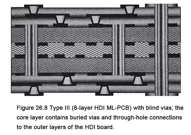
This is particularly relevant for dense designs with blind or buried vias, tight via-in-pad geometries, or fine-pitch BGA fanout patterns. These structures push against process limits in ways that generic DRC rules are not equipped to evaluate. A fabricator's engineering team, reviewing the same design, will immediately recognize the risk. The design tool, running its checks, will not.
How Design Rule Interpretations Diverge
Another underappreciated source of verification failure is the inconsistency in how design rules are interpreted across different tools and different fabricators. IPC standards provide a common framework, but they leave substantial room for interpretation—and fabricators make their own engineering judgments about what they will and will not build.
A design rule defined as a minimum in one tool may be treated as a target by another. A clearance that one fabricator considers achievable in standard production may require a premium process tier at a different shop. When engineers import design rule files from fabricator websites without scrutinizing the assumptions embedded in those files, they may be running checks against a rule set that does not actually reflect what that fabricator will accept.
The safest practice is to request a design rule review directly from the fabricator's engineering team before finalizing a layout—not after. Many US fabricators offer pre-production design reviews as a standard service. Using that service consistently, rather than treating it as a last resort when problems arise, is one of the most effective ways to close the verification gap.
Practical Strategies for Closing the Gap
No design tool, regardless of how advanced, will fully replicate the judgment of an experienced fabrication engineer reviewing a real design against a real process. Accepting that limitation is the starting point for a more disciplined verification approach.
Several practical strategies follow from that acceptance. First, establish relationships with your fabricators before design begins—not when Gerbers are ready to ship. Obtain their process capability documents, their preferred stackup configurations, and their design rule recommendations in their own terms. Build your design constraints around those specifics.
Second, treat DFM review as a mandatory step in the design flow rather than an optional courtesy. Whether that review comes from an internal manufacturing engineer, a contract manufacturer, or the fabricator's own team, it should happen before tape-out, not after.
Third, when evaluating new fabricators or new process capabilities, build test vehicles that probe the specific tolerances your design depends on. Controlled-impedance test coupons, via chain structures, and fine-pitch test patterns give you real data about a fabricator's process—data that no software model can substitute for.
Finally, resist the temptation to treat a clean DRC output as a green light for production. It is, at best, a necessary condition. The sufficient condition is a design that has been reviewed against the actual capabilities of the shop that will build it.
The Cost of Misplaced Confidence
The verification gap is not a software failure. EDA tools are doing exactly what they are designed to do. The failure is in treating those tools as a complete substitute for manufacturing knowledge—and in treating the factory floor as a black box that should simply execute whatever the software approves.
For American electronics teams operating in a competitive environment where schedules are tight and prototype costs are significant, the price of a failed manufacturability review is real: delayed launches, unexpected respins, and engineering hours spent diagnosing problems that earlier engagement would have prevented. Closing the gap between design-tool verification and fabrication reality is not a technical challenge. It is a process discipline challenge—and the teams that take it seriously consistently produce better outcomes than those that do not.