Inside the Stack: How Buried Via Technology Is Quietly Rewriting the Economics of High-Density PCB Design
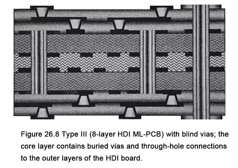
Photo: multilayer PCB cross section buried via HDI manufacturing close up, via www.fastturnpcbs.com
For much of the past two decades, the buried via sat at the edge of most American PCB engineers' awareness — acknowledged as a powerful tool, yet consistently left off the bill of materials. The reasons were practical: higher fabrication costs, limited domestic supplier options, and a manufacturing ecosystem that often penalized complexity at the lamination stage. The result was a persistent tradeoff between routing density and budget that constrained product design in ways many teams never fully examined.
That tradeoff is now under serious pressure. Advances in sequential lamination processes, improved laser drilling precision, and the maturation of domestic high-density interconnect (HDI) fabrication have collectively changed what is achievable — and at what price point. For engineering teams willing to revisit assumptions formed in an earlier era of American PCB manufacturing, the buried via is no longer a premium indulgence. In many cases, it is becoming the economically rational choice.
What a Buried Via Actually Does — and Why It Matters
To understand the economic argument, it helps to start with the engineering fundamentals. A buried via connects two or more internal layers of a multilayer PCB without penetrating the outer surfaces of the board. Unlike a through-hole via, which consumes vertical real estate across every layer of the stackup, a buried via occupies space only where it is needed. This distinction is not cosmetic. In high-density designs — particularly those incorporating fine-pitch BGAs, tight component spacing, or demanding signal integrity requirements — the ability to route connections internally without consuming surface or outer-layer routing channels can be the difference between a manufacturable board and one that requires a layer count increase to resolve congestion.
Blind vias, which connect an outer layer to one or more inner layers without passing through the full board, offer a related capability. Together, these interconnect strategies form the foundation of HDI design, enabling engineers to pack more functionality into a given board area while maintaining controlled impedance and manageable layer counts.
The Old Cost Equation and Why It No Longer Holds
The conventional wisdom held that buried vias added significant cost due to the sequential lamination process they require. A standard multilayer board is laminated in a single pressing cycle. A board with buried vias must be partially laminated, drilled, plated, and then laminated again — a sequence that introduces additional process steps, increases cycle time, and historically required specialized fabrication equipment that fewer domestic shops maintained.
That equipment gap has narrowed considerably. A growing number of American PCB manufacturers have invested in laser drilling systems and sequential lamination capabilities over the past several years, driven in part by domestic demand from defense, medical device, and advanced consumer electronics sectors. The result is a more competitive supplier landscape that has applied downward pressure on the fabrication premium associated with buried via boards.
More importantly, engineering teams are beginning to conduct more rigorous total-cost comparisons. When a design that would otherwise require twelve or fourteen layers can be executed in eight layers using buried vias, the layer count reduction generates its own cost savings — in raw material, fabrication complexity, board weight, and assembly yield. The premium for sequential lamination, when weighed against the savings from a reduced layer count, frequently narrows to a fraction of what the headline fabrication quote suggests.
Real-World Routing: Where the Density Argument Becomes Concrete
Consider the challenge facing a hardware team developing a compact industrial controller incorporating a high-pin-count processor, multiple memory interfaces, and a dense power delivery network. In a conventional through-hole via strategy, escape routing from fine-pitch BGA packages consumes outer-layer routing channels aggressively, often forcing the design into additional layers simply to achieve clean signal separation. Fanout becomes a bottleneck that cascades through the entire stackup.
With buried vias available for internal escape routing, the same design can achieve BGA fanout on inner layers, preserving outer-layer channels for power planes and critical signal traces. Engineers at several US-based hardware firms have reported layer count reductions of two to four layers on comparable designs when moving from a through-hole-only via strategy to an HDI approach incorporating buried and blind vias. At current domestic fabrication pricing, a two-layer reduction on a mid-volume production run can represent a per-board cost savings that more than offsets the HDI fabrication premium within the first production release.
The Reliability Dimension
Cost economics are not the only argument shifting in favor of buried vias. Reliability data accumulated from aerospace, defense, and medical device applications — sectors that adopted HDI technology earlier than commercial electronics — consistently demonstrates that buried vias, when properly designed and fabricated, exhibit superior mechanical reliability compared to full-depth through-hole vias under thermal cycling conditions.
The physics are straightforward. A through-hole via spanning the full thickness of a twelve-layer board is subject to significant z-axis stress during thermal excursions. The copper barrel must accommodate the cumulative expansion of all intervening dielectric material. A buried via spanning only two or three internal layers faces a fraction of that mechanical demand. In applications where long-term field reliability is a design requirement — industrial equipment, automotive electronics, medical instrumentation — this distinction carries real weight in the risk calculus.
What Forward-Thinking Teams Are Doing Differently
The engineering teams deriving the most value from buried via technology share a common characteristic: they are engaging with fabrication constraints at the schematic and stackup definition stage, not after the layout is substantially complete. This earlier integration of manufacturing awareness allows the design to be structured around the capabilities of the chosen fabrication process from the outset, rather than retrofitted to accommodate HDI requirements late in the cycle.
This approach requires closer collaboration between design engineers and PCB fabricators than the traditional arm's-length relationship that characterized much of American electronics manufacturing in the outsourcing era. As domestic fabrication relationships strengthen — a trend accelerated by supply chain resilience initiatives and the reshoring of electronics production — the conditions for this kind of early-stage collaboration are improving.
Rethinking the Default
The buried via is no longer a technology that requires a special justification to appear on a design. For an expanding range of American PCB projects — particularly those involving fine-pitch components, density constraints, or long-term reliability requirements — it is becoming the approach that requires no justification at all. The question engineering teams should be asking is not whether buried vias are worth the premium, but whether the assumptions underlying that premium were ever as durable as they seemed.
As domestic HDI fabrication capacity continues to develop and total-cost comparisons become more rigorous, the answer is increasingly clear. The economics have shifted. The design freedom that buried vias enable has always been real. Now, for the first time in the mainstream American market, the cost structure is beginning to reflect that reality.