Trace Width Errors: The Hidden Fault Line Between Prototype Success and Production Failure
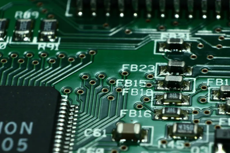
There is a particular kind of engineering frustration that arrives not during development, but after it. A prototype clears every bench test, impresses stakeholders, and earns sign-off for full production—only to fail repeatedly once manufacturing scales. The root cause, when investigators finally trace it back, is often something that appears mundane on a schematic: a trace that is fractionally too narrow, or a current-carrying conductor that was never properly validated against real-world thermal loads.
Trace width miscalculation is among the most consequential and least dramatic errors in PCB design. It does not announce itself with sparks or smoke during prototyping. It accumulates quietly, expressing itself only when production volumes, tighter manufacturing tolerances, and real operating environments converge.
Why Prototypes Mask the Problem
Prototype PCBs are typically fabricated under controlled, often premium conditions. Small-batch fabricators apply tighter tolerances, operators handle boards with greater care, and the test environment rarely replicates the thermal cycling, vibration, or sustained current draw of a deployed product. Under these forgiving conditions, a trace that is five to ten percent narrower than it should be may carry current without visible distress.
The transition to volume manufacturing changes every variable simultaneously. Fabrication tolerances widen. Etch variation across larger panels introduces dimensional inconsistency. Boards that passed prototype testing begin failing incoming inspection, or worse, pass inspection and fail in the field.
A defense electronics subcontractor based in the Midwest learned this distinction painfully several years ago when a communication module that had completed eighteen months of prototype validation failed thermal screening at a rate exceeding thirty percent during its first production run. Post-failure analysis identified trace widths on high-current power rails that had been calculated using IPC-2221 tables without accounting for the reduced copper weight specified by the volume fabricator. The discrepancy was less than two mils. The rework cost exceeded four hundred thousand dollars.
The Calculation Gap: Where Engineers Go Wrong
Trace width is governed by a deceptively simple relationship: current capacity, copper thickness, allowable temperature rise, and ambient operating temperature. IPC-2221 and its successor standards provide lookup tables and formulas that are widely used and broadly trusted. The problem is not that these standards are incorrect—it is that engineers frequently apply them incompletely.
Several recurring errors appear consistently in production failure investigations:
Assuming uniform copper weight. Design files may specify one-ounce copper, but fabricators working within cost constraints may deliver boards at the lower end of the tolerance band. A trace calculated for one-ounce copper that receives 0.9-ounce copper will carry proportionally less current before reaching its thermal limit.
Ignoring adjacent trace heating. High-density layouts concentrate heat. A trace that would dissipate safely in isolation may exceed its thermal budget when surrounded by other current-carrying conductors operating simultaneously. Thermal interaction between traces is rarely captured in single-trace calculations.
Failing to account for surface finish variation. HASL, ENIG, and OSP surface finishes affect effective conductor geometry in ways that are small individually but meaningful in aggregate, particularly on fine-pitch designs.
Treating inner and outer layers as equivalent. Inner-layer traces dissipate heat through the dielectric rather than into ambient air. IPC-2221 provides separate correction factors for internal conductors, and they are not always applied.
What Simulation Can—and Cannot—Do
Modern PCB design environments offer thermal simulation tools capable of modeling current density, resistive heating, and temperature distribution across a layout. These tools, when used correctly, can identify problematic traces before a single board is fabricated. Platforms such as Cadence Celsius, Ansys Icepak, and Zuken's thermal analysis modules have become increasingly accessible to mid-sized design teams.
However, simulation accuracy depends entirely on the quality of input data. A thermal model built on nominal copper weights, idealized boundary conditions, and assumed ambient temperatures will produce optimistic results that may not survive contact with a production environment. Simulation is a powerful verification tool, not a substitute for conservative design margins.
The most effective approach treats simulation as one layer of a multi-stage verification process rather than a final authority. Simulation identifies candidates for concern. Engineering judgment and empirical testing validate the findings.
Building a Verification Checklist That Actually Works
Verification checklists are common in electronics manufacturing. They are also commonly ineffective, because they are built to confirm that work was done rather than to challenge whether it was done correctly. A checklist that asks "were trace widths calculated?" provides no protection. A checklist that asks "were trace widths calculated using the copper weight and tolerance band specified by the volume fabricator, with thermal derating applied for adjacent conductors?" is a different instrument entirely.
An effective pre-production trace verification protocol should include the following elements:
- Fabricator-specific tolerance review. Obtain the actual copper weight tolerance band from the intended volume fabricator and recalculate critical traces using the minimum value within that band.
- Thermal adjacency assessment. Identify all traces operating above fifty percent of their calculated current capacity and evaluate each in the context of neighboring conductors.
- Layer-specific derating. Apply IPC-2221 internal-layer correction factors to all inner conductors carrying meaningful current, without exception.
- Worst-case ambient temperature modeling. Calculate trace performance at the maximum operating temperature specified in the product's environmental requirements, not at room temperature.
- Cross-functional sign-off. Require both the design engineer and the manufacturing engineer to independently review trace width calculations on all power-carrying nets before design release.
The Cost Argument for Getting It Right Early
Engineering discipline has a financial dimension that is sometimes difficult to quantify in advance but becomes painfully legible after a production failure. Tooling costs for a mid-complexity PCB can reach tens of thousands of dollars. A production run that must be scrapped due to systematic trace failures can represent months of lost revenue and, in regulated industries, potential contractual penalties.
Against this backdrop, the investment in rigorous trace width verification is not a quality expense—it is a risk management decision with a calculable return. An engineering team that spends two additional days verifying trace calculations before design release is purchasing insurance against outcomes that can consume an entire program's margin.
At PCBs Inv, we have observed that the firms consistently achieving clean prototype-to-production transitions share a common characteristic: they treat manufacturability as a design constraint from the first schematic capture, not as a checklist item appended at the end of the development cycle. Trace width is not a detail to be revisited at design review. It is a foundational parameter that determines whether a product can be built reliably at scale.
The silent saboteur is not difficult to defeat. It simply requires the discipline to look for it before the production line makes the search unavoidable.