Water's Quiet War on Electronics: Engineering Moisture Out of Your PCB Before It Costs You
Electronics engineers spend considerable effort optimizing signal integrity, thermal performance, and component placement. Yet one of the most destructive forces acting on a finished circuit board is invisible, odorless, and relentlessly patient: moisture. Whether it enters during manufacturing, shipping, storage, or years into a product's service life, water vapor is responsible for a disproportionate share of field failures—many of which are misattributed to component defects or design errors long after the real cause has evaporated.
For American manufacturers serving industries from industrial automation to consumer electronics, understanding moisture ingress is not optional. It is foundational.
How Moisture Compromises a Circuit Board
Water is a polar molecule, and that polarity makes it extraordinarily effective at disrupting the electrochemical environment of a PCB. When humidity penetrates a board, it does not simply sit on the surface. It migrates into micro-voids within the laminate, travels along fiber-resin interfaces in the substrate, and accumulates beneath component packages where cleaning solutions rarely reach.
The consequences unfold along several pathways. Electrochemical migration—sometimes called dendritic growth—occurs when dissolved ionic contaminants travel between conductors under an applied voltage, eventually forming conductive filaments that create short circuits. Conductive anodic filament (CAF) formation is a related phenomenon, propagating through the glass fiber bundles of FR4 laminates and bypassing the insulation entirely.
Corrosion is another mechanism. Copper traces oxidize when exposed to moisture combined with residual flux or ionic contamination from the manufacturing process. Over time, this oxidation increases resistance at joints and vias, introducing signal degradation that can be nearly impossible to trace without physical cross-sectioning.
Finally, moisture absorption causes mechanical stress. Laminate materials expand and contract with humidity cycling, and in assemblies with mixed-material components—ceramic capacitors mounted on organic substrates, for instance—differential expansion generates micro-cracking at solder joints. In field environments that experience seasonal temperature swings, this process accelerates dramatically.
The American Climate Problem
The United States presents a uniquely challenging operating environment for deployed electronics. A control board installed in a Gulf Coast industrial facility faces sustained heat and near-saturation humidity for months at a time. The same board design installed in a Minnesota agricultural operation must survive sub-zero winters followed by humid spring thaws. Electronics in Pacific Northwest data centers contend with persistent ambient moisture, while desert Southwest installations deal with UV exposure combined with occasional monsoon humidity spikes.
This geographic diversity means that a design validated in a controlled laboratory environment may fail within eighteen months in the field. Engineers who treat moisture resistance as a single-pass checkbox—rather than a climate-specific engineering discipline—routinely discover this the hard way.
Substrate and Material Selection
Moisture management begins at the material selection stage, long before a layout file is finalized. Standard FR4 laminate absorbs moisture at a rate that varies significantly between manufacturers and grades. High-performance alternatives such as Rogers 4000 series laminates, polyimide substrates, and low-loss PTFE-based materials offer substantially reduced moisture absorption coefficients. For applications where long-term reliability in humid environments is a design requirement, specifying a low-Dk, low-moisture-absorption laminate is one of the highest-leverage decisions an engineer can make.
Via design also plays a role. Blind and buried vias, when improperly processed, can trap moisture and cleaning chemistry inside the barrel. Specifying tented vias—covered with solder mask on one or both sides—reduces the exposed surface area that moisture can penetrate. For high-reliability applications, filled and capped vias eliminate the internal cavity entirely.
Conformal Coating as a Defense Layer
Conformal coatings are the most widely deployed moisture barrier in the electronics industry, and for good reason: applied correctly, they form a continuous polymer film over the board surface that dramatically reduces the rate of moisture ingress. The key word is correctly.
Acrylic coatings are the most common choice due to their ease of application and reworkability. They perform well in moderate humidity environments and offer good protection against condensation. Silicone coatings excel in extreme temperature applications—both high and low—and maintain flexibility across a wider thermal range. Polyurethane coatings offer superior abrasion resistance and chemical protection, making them well-suited to industrial and automotive environments. Epoxy coatings provide the hardest barrier but are difficult to rework and may crack under thermal cycling.
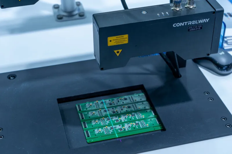
Application method matters as much as chemistry. Selective coating systems, which apply material only to designated areas while masking connectors and test points, have become the manufacturing standard for high-volume boards. Dip coating and spray coating remain viable for lower-complexity assemblies. In all cases, achieving consistent film thickness—typically between 25 and 75 micrometers—is critical. Thin spots create vulnerability; thick spots can trap solvents and cause adhesion failures.
Design Practices That Reduce Exposure
Beyond materials and coatings, layout decisions directly affect moisture vulnerability. Minimizing the spacing between high-voltage conductors reduces the distance that conductive filaments must travel to create a short circuit, while maximizing spacing—where layout rules permit—increases the margin of safety. Specifying appropriate solder mask coverage over copper features reduces the bare metal surface exposed to the environment.
Component orientation matters in wave-soldering and selective-soldering processes, where shadowing effects can leave flux residues trapped beneath components. Those residues, when combined with moisture, become ionic contamination sources. Orienting components to minimize shadowing—or specifying reflow-only processes for moisture-sensitive assemblies—reduces post-process contamination risk.
Enclosure design, while outside the PCB layout itself, is part of the system-level moisture strategy. Specifying IP-rated enclosures, incorporating desiccant packets in sealed assemblies, and designing cable entry points with appropriate strain relief and sealing gaskets are all elements of a complete moisture management approach.
Baking and Handling Protocols
Moisture damage does not always originate in the field. Moisture-sensitive components—particularly plastic-encapsulated ICs and ball grid array packages—absorb ambient humidity during storage. When subjected to reflow oven temperatures, that trapped moisture vaporizes rapidly, generating internal pressure that causes delamination, cracking, or what the industry calls "popcorning."
IPC/JEDEC J-STD-020 establishes moisture sensitivity levels (MSL) for components, and adherence to these standards during incoming inspection, storage, and production is non-negotiable for high-reliability manufacturing. Components rated MSL 3 or higher must be stored in dry-pack conditions and baked prior to assembly if their floor life has been exceeded. Many field failures that appear as solder joint defects originate at this stage.
Building Reliability In, Not Testing It Out
The electronics industry has a long tradition of attempting to validate reliability through end-of-line testing rather than engineering it into the design. Moisture-related failures expose the limits of that approach. A board that passes all functional tests on the day it ships may fail eighteen months later in a Florida equipment room, not because something changed in the design, but because the design never accounted for sustained humidity exposure.
At PCBs Inv, we believe that reliability is an engineering output, not a quality inspection outcome. Treating moisture ingress as a first-class design constraint—addressed at the substrate selection stage, reinforced through layout decisions, and sealed with an appropriate coating strategy—is the difference between a product that performs across its full service life and one that generates warranty claims and customer attrition.
The tools and materials to design moisture out of a circuit board exist today. The question is whether engineers choose to use them before the first unit ships, or after the first field failure report arrives.