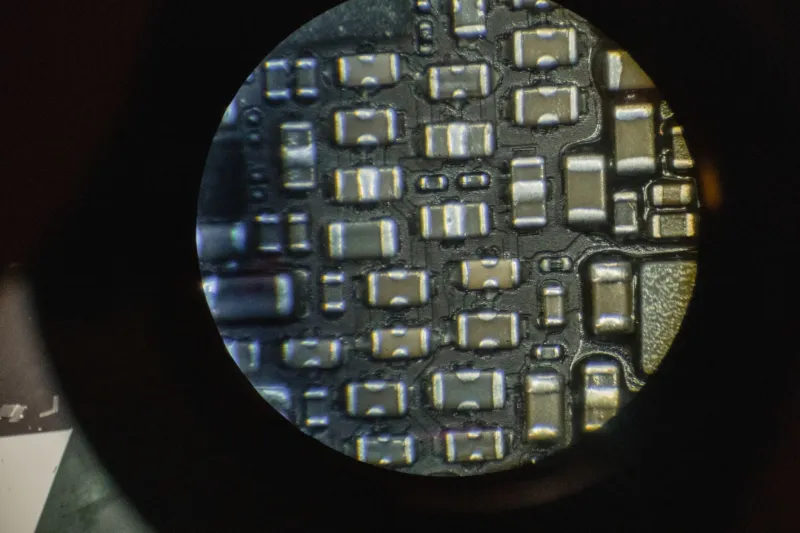
Cracking Under Pressure: The Solder Joint Fatigue Crisis Hidden Inside Every Device You Own
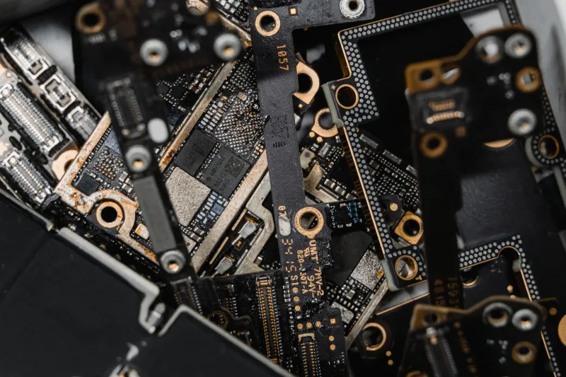
Every time you pull your smartphone from your pocket, slide it onto a car seat, or leave it on a sun-baked dashboard, you are subjecting its internal solder joints to a punishment they were never designed to absorb indefinitely. The damage is invisible, incremental, and relentless. By the time a device fails—a flickering screen, an intermittent connection, a sudden shutdown—the underlying solder joint has likely been accumulating microcracks for months or even years. This is the quiet crisis of solder joint fatigue, and it is actively shortening the useful life of electronics across virtually every consumer and industrial category.
The Mechanics of an Invisible Failure
Solder joints serve a dual purpose in printed circuit board assemblies: they establish electrical continuity between components and their pads, and they provide mechanical anchoring to the board itself. Under ideal, static conditions, a properly formed solder joint is more than adequate for both roles. Real-world conditions, however, are anything but static.
Thermal cycling is the primary aggressor. Every time a device powers on and off, or moves between environments of differing temperature, the materials within the assembly expand and contract at different rates. Copper, FR-4 laminate, silicon die, and solder alloy each carry distinct coefficients of thermal expansion. This mismatch generates shear stress at the solder interface with every thermal event. Individually, each stress cycle is negligible. Cumulatively, over thousands of power cycles and environmental transitions, the stress accumulates through a process engineers call thermomechanical fatigue.
Vibration compounds the problem considerably. A device carried in a pocket experiences continuous low-amplitude vibration from walking, transit, and handling. Ball grid array packages, which dominate modern high-density designs, are particularly susceptible because their solder balls bear the full mechanical load between a rigid component body and a relatively flexible PCB substrate. The outermost corner balls on a BGA package absorb disproportionate stress during both thermal cycling and dynamic flexure, and failure analysis data consistently identifies these locations as the earliest sites of crack initiation.
Why Traditional Design Approaches Miss the Warning Signs
The frustrating reality for many engineering teams is that solder joint fatigue failures rarely appear during standard qualification testing. Accelerated thermal cycling protocols, such as those specified under IPC-9701 or JEDEC standards, are designed to detect gross reliability deficiencies—not to replicate the nuanced fatigue accumulation that occurs across a device's actual service life in consumer hands.
Furthermore, schematic-phase design reviews almost never incorporate solder joint fatigue as a first-order design constraint. Component placement, thermal management, and signal integrity dominate early design conversations, while the mechanical behavior of solder interfaces is typically deferred to later layout stages—or addressed only after field failures prompt a retrospective analysis. By that point, the design is committed, tooling is complete, and corrective options are expensive.
Board-level mechanical simulation tools have existed for years, but their adoption in consumer electronics development cycles has been inconsistent. Many smaller US design houses lack the in-house expertise to run finite element analysis models that accurately predict fatigue life under combined thermal and vibration loading. The result is a persistent gap between what engineers could know and what they actually account for during development.
Predicting Fatigue Life Before a Single Board Is Built
The good news is that the tools and methodologies for early-stage fatigue life prediction have matured considerably. Engineers willing to invest in simulation during the schematic and pre-layout phases can now generate meaningful reliability forecasts that directly inform component selection, PCB stackup decisions, and pad geometry specifications.
Coffin-Manson fatigue models, adapted for solder alloy behavior, allow designers to estimate the number of thermal cycles a joint can withstand before crack propagation reaches a critical threshold. More sophisticated approaches, including Anand viscoplastic constitutive models, account for the creep behavior of solder under sustained stress—a critical consideration for devices operating in high-temperature environments such as automotive interiors or outdoor industrial enclosures.
Practical design interventions derived from these analyses include increasing solder mask defined pad geometries to reduce stress concentration, adjusting component standoff heights to distribute shear loads more evenly, and selecting underfill materials for BGA packages in applications where vibration exposure is expected to be severe. Even the orientation of elongated components relative to the primary axis of board flexure can meaningfully alter fatigue outcomes.
For US-based manufacturers operating under tight development timelines, the most accessible entry point is often a partnership with a contract manufacturer or third-party reliability engineering firm that maintains simulation infrastructure and failure analysis capabilities. The upfront investment is substantially smaller than the cost of a field recall or a warranty replacement program triggered by solder fatigue failures at scale.
Solder Alloy Innovation: Beyond the Cost-Cutting Narrative
The transition from tin-lead to lead-free solder alloys, driven by RoHS compliance requirements, introduced a reliability challenge that the industry is still actively resolving. SAC305—the tin-silver-copper alloy that became the default lead-free standard—exhibits lower ductility and higher stiffness than traditional tin-lead solder. Under thermal cycling, this translates to faster crack propagation and shorter fatigue life in certain application profiles, particularly those involving aggressive temperature swings.
In response, a new generation of solder alloy formulations has emerged with a focus on genuine reliability improvement rather than cost reduction alone. Alloys incorporating small additions of bismuth, antimony, or indium have demonstrated measurable improvements in thermal fatigue resistance. Some formulations, including those marketed under proprietary designations by suppliers such as Indium Corporation and Alpha Assembly Solutions, show fatigue life improvements of 30 to 50 percent over standard SAC305 in standardized thermal cycling tests.
American electronics manufacturers in sectors where longevity is non-negotiable—defense electronics, medical devices, industrial control systems—have been early adopters of these advanced alloys. Consumer electronics has been slower to follow, partly because per-unit material cost differentials are scrutinized intensely at production volumes of millions of units. However, as device replacement cycles lengthen and sustainability expectations increase among US consumers, the economic calculus is beginning to shift. A device that lasts three years instead of eighteen months represents both a warranty cost reduction and a brand differentiation opportunity that is increasingly difficult to ignore.
Designing With Longevity as the Objective
Solder joint fatigue will never be fully eliminated—it is a consequence of the physical laws governing thermal expansion and material behavior under cyclic stress. What can be changed is the degree to which engineers treat it as an afterthought rather than a primary design constraint.
The most resilient PCB assemblies being produced in the United States today share a common characteristic: their designers engaged with mechanical reliability questions at the earliest possible stage of development. They ran thermal models before committing to component placement. They evaluated solder alloy options alongside component cost negotiations. They specified underfill or corner bonding as standard practice for high-stress package configurations rather than as a remediation measure applied after failures surfaced.
The devices most at risk are those designed under the assumption that a solder joint is simply a solder joint—an interchangeable electrical connection that requires no further engineering consideration. That assumption has always been incorrect. In an era of increasingly dense, increasingly powerful, and increasingly portable electronics, it is a mistake that the industry can no longer afford to make quietly.