Smaller Is Not Always Smarter: The Hidden Costs of Chasing Advanced Lithography in PCB Manufacturing
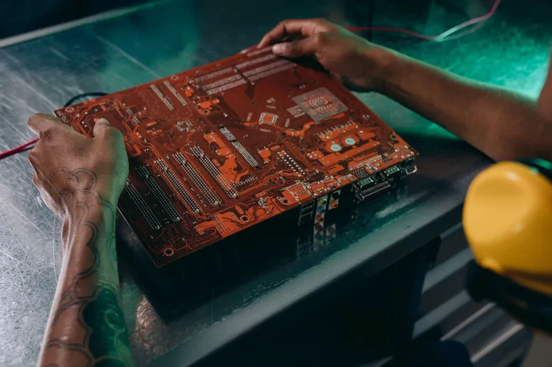
For decades, the electronics industry has operated under a powerful assumption: smaller process nodes produce better results. Moore's Law, shrinking transistor geometries, and the relentless cadence of semiconductor advancement have all reinforced the idea that newer lithography equals superior performance. Yet on the PCB manufacturing floor, that assumption is quietly generating a category of failure that few engineering teams openly discuss — and even fewer budget for.
The truth is more nuanced, and for American electronics manufacturers competing in cost-sensitive, high-reliability markets, understanding when to pursue advanced lithography and when to rely on proven processes is no longer optional. It is a strategic imperative.
What Lithography Promises — and What It Delivers
Advanced lithography in PCB contexts typically refers to fine-line trace manufacturing, tighter via tolerances, and the integration of semiconductor-grade patterning techniques into board-level production. The theoretical benefits are genuine: denser routing, reduced parasitics, and the ability to support increasingly compact component footprints. In high-frequency RF and millimeter-wave applications, tighter geometries can meaningfully improve signal performance.
But the gap between theoretical benefit and production reality is where engineering teams tend to lose ground. Fine-line processes demand tighter process controls, specialized equipment, and substrates that behave consistently across temperature, humidity, and mechanical stress cycles. When any one of those variables drifts — as they inevitably do in volume production — the failure modes that emerge are neither predictable nor inexpensive to diagnose.
Several US defense contractors and commercial electronics firms have encountered this firsthand. Engineering teams that specified advanced node processes to gain marginal density improvements found themselves managing yield losses that erased the projected cost savings within the first production run. The boards passed simulation. They passed early prototyping. They failed at scale.
The Manufacturability Problem Nobody Talks About
One of the most persistent gaps in PCB engineering culture is the tendency to evaluate lithographic capability in isolation from the full manufacturing ecosystem. A process node that a fabricator can execute reliably under controlled laboratory conditions may behave entirely differently when exposed to the thermal cycling of a reflow oven, the mechanical stress of depaneling, or the chemical variability of a high-volume plating line.
Fine-line traces — particularly those approaching 2-mil widths or tighter — are especially vulnerable to copper grain structure inconsistencies that emerge during electroplating. These inconsistencies do not always manifest as visible defects. Instead, they create localized impedance variations that only surface during high-speed signal testing or, worse, after deployment in the field.
The situation is compounded by the fact that most standard DFM (Design for Manufacturability) review processes were not built to interrogate advanced lithographic constraints with the same rigor they apply to drill registration or solder mask clearances. Engineers who rely on automated DFM checks to validate cutting-edge process choices are, in effect, using yesterday's tools to evaluate tomorrow's problems.
When Older Processes Outperform Newer Ones
This is the conversation that rarely appears in trade publications or vendor presentations: mature, well-characterized process nodes frequently outperform their advanced counterparts in real-world production environments.
Consider standard 4-mil trace-and-space processes, which have been refined over decades of volume production across hundreds of domestic fabricators. The process windows are wide, the failure modes are well understood, and the yield data is deep. An engineering team that designs to these tolerances benefits from a manufacturing ecosystem that has already solved most of the problems that advanced processes are still generating.
For the majority of commercial PCB applications — industrial controls, medical instrumentation, power electronics, embedded systems — the performance delta between a mature 4-mil process and a cutting-edge 2-mil process is negligible. The functional requirements simply do not demand the tighter geometry. Yet procurement decisions, competitive pressure, and a cultural bias toward technological novelty continue to push teams toward specifications their supply chains are not fully equipped to support.
Signal Integrity: Where Node Shrinking Can Actually Hurt
Perhaps the most counterintuitive finding from engineering teams that have stress-tested advanced lithographic processes is the signal integrity degradation that can accompany trace miniaturization.
Narrower traces exhibit higher resistance per unit length, which matters significantly in power delivery networks and high-current signal paths. More critically, the tighter via structures that accompany advanced node designs can introduce stub resonances and impedance discontinuities that are extraordinarily difficult to model accurately before fabrication. Electromagnetic simulation tools are improving, but they still struggle to account for the full range of material and process variability present in high-volume production.
The result is a class of signal integrity problem that appears only after boards are built — a phenomenon that compounds testing cycles, extends project timelines, and generates the kind of cost overruns that damage program budgets and supplier relationships simultaneously.
A Framework for Making the Right Process Decision
The goal is not to reject advanced lithography categorically. There are genuine applications where tighter process nodes are not merely beneficial but necessary — phased-array radar systems, millimeter-wave communications hardware, and certain high-density server interconnects among them. The discipline lies in applying those processes selectively, with full visibility into the manufacturing constraints they impose.
Engineering teams that consistently make sound process decisions tend to follow a structured evaluation approach. They begin by asking whether the functional requirement actually demands the tighter geometry, or whether the specification is driven by assumption. They engage fabricators early in the design cycle, before layout decisions are locked, to understand the realistic process windows available in production — not in a prototype lab. And they build yield risk into their program economics, rather than treating advanced process capability as a zero-cost upgrade.
This discipline is particularly important for US manufacturers navigating the current domestic production landscape. As American fabricators invest in modernizing their process capabilities, the temptation to specify the newest available technology will only intensify. Engineering teams that can distinguish between genuine performance requirements and technological novelty will build more reliable products, hit production schedules more consistently, and protect the program margins that keep development pipelines funded.
The Competitive Advantage of Process Wisdom
The most capable PCB engineering organizations in the United States are not necessarily those chasing the leading edge of lithographic technology. They are the ones that have developed the institutional knowledge to match process selection to application requirements with precision — knowing when mature processes deliver superior outcomes and when advanced nodes are genuinely warranted.
That judgment cannot be automated, and it cannot be purchased from a tool vendor. It is built through accumulated manufacturing experience, close supplier relationships, and a willingness to question the assumption that smaller always means better. In a competitive market where reliability and time-to-production are decisive differentiators, process wisdom may be the most valuable engineering asset a team can develop.