From Bench to Factory Floor: Why Prototype Success Means Nothing Until Production Proves It
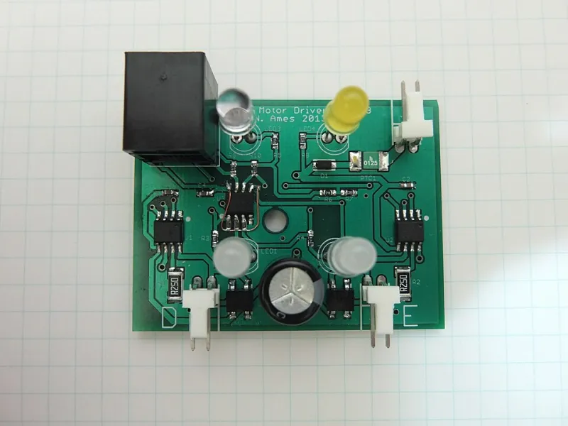
Photo: Nick Ames, CC BY-SA 2.0, via Wikimedia Commons
There is a particular kind of confidence that settles over an engineering team when a prototype clears every test on the bench. Signal integrity checks out. Thermal performance holds. The firmware boots cleanly and the board behaves exactly as designed. After weeks or months of iteration, that moment of validation feels definitive.
It is not.
For engineers who have spent careers in PCB development and volume manufacturing, the gap between a working prototype and a reliably manufacturable product represents one of the most treacherous stretches in the entire product development cycle. Boards that pass every qualification test in a controlled lab environment can—and frequently do—generate yield collapses, field failures, and costly production holds the moment they encounter real-world manufacturing conditions at scale. Understanding why requires a close examination of what prototype validation actually measures, and what it almost never does.
The Illusion of the Perfect Prototype
Prototype builds are, by definition, exceptions. A skilled technician assembles a small quantity of boards under careful supervision, often with hand-selected components, manually adjusted process parameters, and the kind of individual attention that no production line can replicate across thousands of units per shift.
When that prototype performs well, engineers tend to interpret the result as evidence that the design is sound. In a narrow sense, it is. But manufacturing at scale is not a magnified version of prototype assembly. It is a fundamentally different environment governed by statistical process windows, supplier variability, machine tolerances, and material lot-to-lot inconsistencies that simply do not exist when you are building ten boards in a development lab.
The failure to account for this distinction is not a matter of negligence. It is a structural problem embedded in how most product development timelines are organized. Prototype success is treated as a gate to production readiness, when in reality it should be treated as the beginning of a separate engineering discipline entirely.
Process Windows and the Tolerance Stack Problem
One of the most common sources of production yield failure involves what manufacturers refer to as process window collapse. Every step in PCB assembly—solder paste deposition, reflow profiling, wave soldering, selective soldering, cleaning—operates within a defined range of acceptable parameters. A prototype build often lands near the center of those windows, where everything works comfortably.
At volume, however, natural variation across machines, operators, shifts, and environmental conditions pushes individual boards toward the edges of those windows. When a design carries tight tolerances in multiple interdependent parameters simultaneously, the probability that any given board lands outside at least one of those windows rises sharply. This is the tolerance stack problem, and it is invisible during prototype validation.
Consider a high-density board with fine-pitch components, aggressive via-in-pad geometry, and a lead-free reflow profile optimized for a specific laminate material. On the bench, that combination works. In production, the same combination may generate inconsistent solder joint formation under the thermal gradients of a conveyor oven, voiding beneath BGA packages that only becomes visible under X-ray inspection—or worse, in the field.
Material Substitution and the Laminate Lottery
Prototype builds frequently use premium laminate materials sourced from preferred suppliers with tightly controlled dielectric properties. Production builds, particularly during periods of supply constraint, often do not. When procurement substitutes a functionally equivalent laminate from a different manufacturer—or even a different production lot from the same manufacturer—the resulting variation in Dk values, moisture absorption rates, and thermal expansion coefficients can shift impedance-controlled traces outside specification, alter via drill quality, and affect the reliability of plated through-holes under thermal cycling.
This is not a hypothetical scenario. American electronics manufacturers have documented cases where yield rates on impedance-critical boards dropped by 15 to 30 percent following a laminate substitution that passed every incoming inspection criterion. The engineering team had validated the design against one material. The production floor was building it with another.
The solution is not simply to lock in a single approved supplier, though that helps. It is to design with material variation explicitly modeled into the specification—to understand the performance envelope of the design across the realistic range of materials that production will encounter, not just the ideal material used in development.
Component Variation at Volume
Individual prototype builds often draw from engineering sample inventory or carefully selected production stock. At volume, components arrive in production reels from distribution channels that may include parts from multiple manufacturing lots with legitimate but non-trivial parametric variation.
Passive components—resistors, capacitors, inductors—carry tolerance ratings that are well understood in theory but frequently underestimated in practice when they interact with each other across a populated board. A circuit designed with tight margins may function correctly when every component lands at its nominal value but begin to exhibit out-of-spec behavior when a subset of components, each within its own tolerance band, combine in an unfavorable configuration. Prototype builds rarely surface this failure mode because the sample size is too small to generate the statistical distribution that volume production will inevitably produce.
Robust design practice requires margin analysis that accounts for worst-case component stacking, not just nominal performance. This analysis is often skipped during prototype development and almost never validated until yield data from early production runs forces the issue.
The DFM Conversation That Happens Too Late
Design for Manufacturability reviews are widely recognized as best practice in electronics development. They are also widely deferred. The most common pattern in US electronics firms is a DFM review that occurs after the prototype has been validated and the design is considered functionally complete—at which point any feedback that requires layout changes is met with resistance because the team has already invested heavily in the current revision.
The result is a DFM process that identifies problems without the organizational authority to fix them. Engineers note that a particular via placement creates a solder bridging risk at production volumes. The feedback is logged. The schedule pressure is real. The design goes to production largely unchanged, and the solder bridging emerges exactly as predicted, now costing far more to address than it would have during layout.
The firms that consistently achieve strong prototype-to-production transitions are those that integrate manufacturing engineering into the design process from the first layout revision, not as a final checkpoint before release. That integration requires deliberate process investment and, in many organizations, a cultural shift in how engineering and manufacturing teams relate to one another.
Designing for the Production Reality, Not the Lab Ideal
The practical implication of everything described above is that prototype validation, while necessary, should never be treated as sufficient evidence of production readiness. A board that works in the lab has demonstrated that the design concept is viable. It has not demonstrated that the design can be manufactured reliably, consistently, and economically at the volumes the business requires.
Closing that gap demands a different set of engineering questions. Not just: does this board meet specification? But: does this board meet specification across the full statistical distribution of materials, components, process parameters, and environmental conditions it will encounter in production? Those are harder questions to answer, and they require more time, more analysis, and more collaboration between design and manufacturing teams than most development schedules comfortably accommodate.
The cost of skipping that work, however, is not theoretical. It is measured in yield loss, rework labor, field returns, and the kind of production delays that erode customer relationships and compress margins on programs that were supposed to be profitable.
Prototype success is a beginning. Production readiness is the discipline that follows it.