The Coupling Problem: Why Electromagnetic Crosstalk in Dense PCBs Keeps Defeating Your Simulation Tools
The board passed every simulation. It cleared the design rule check. It survived bench testing with clean signal margins. Then it failed in the field—intermittently, unpredictably, and in ways that took weeks to trace back to a coupling interaction nobody had modeled.
This sequence is becoming more common, not less. As the electronics industry continues compressing functionality into smaller form factors, electromagnetic coupling between adjacent conductors is escalating from a manageable nuisance into a primary failure driver. And the simulation workflows that most engineering teams rely on are, by design, not built to catch it.
What Coupling Actually Is—and Why Density Makes It Worse
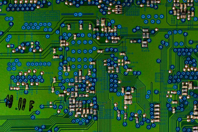
Electromagnetic coupling describes the unintended transfer of energy between conductors that share proximity. Two adjacent signal traces, a trace running parallel to a power plane edge, a via field positioned too close to a high-frequency return path—each of these configurations creates a channel through which electromagnetic energy migrates from one net to another. The result is noise injected into signals that were never supposed to receive it.
Coupling occurs through two primary mechanisms. Capacitive coupling—sometimes called electric field coupling—arises when the electric field surrounding a driven conductor induces charge displacement in a neighboring conductor. Inductive coupling, driven by magnetic field interaction, occurs when the changing current in one conductor generates a voltage in an adjacent loop. In practice, both mechanisms operate simultaneously in most high-density PCB environments, and their combined effect is rarely linear.
Density amplifies both mechanisms. As trace-to-trace spacing decreases, capacitive coupling increases as an inverse function of distance. As signal frequencies rise—a near-universal trend across product categories—inductive coupling intensifies because the rate of current change accelerates. High-density interconnect designs, which routinely push trace widths and spacings below 75 microns, are operating in a regime where coupling effects that were negligible at lower densities become system-defining.
Why Simulations Give Engineers False Confidence
The simulation tools available to PCB engineers today are genuinely sophisticated. 2D and 3D electromagnetic solvers can model field behavior with impressive accuracy—under the right conditions. The problem is that those conditions rarely match the full complexity of a production board.
Most simulation workflows model individual nets or net pairs in isolation. A signal integrity engineer will run a differential pair analysis, confirm that the pair meets eye diagram requirements, and mark the analysis complete. What the simulation does not capture is the behavior of that differential pair when it is surrounded by the actual routing topology of the finished board—adjacent clock lines running at higher frequencies, power delivery network noise coupling through shared reference planes, or via transitions creating impedance discontinuities that radiate into neighboring structures.
Design rule checks compound the problem by giving engineers a binary pass/fail signal that implies safety. A DRC that clears spacing violations confirms that traces are not physically touching and that minimum clearance rules have been met. It says nothing about the electromagnetic interaction between traces that are technically compliant but functionally problematic at the frequencies the design will actually operate.
The gap between what simulation confirms and what the physical board experiences is where coupling failures live.
Field Failures That Bench Testing Missed
Several documented failure cases illustrate the gap between simulation confidence and field reality.
In one communications hardware application, a high-speed serial interface operating at 10 Gbps exhibited intermittent bit error rate degradation after deployment in installations with elevated ambient temperature. Bench testing at room temperature had shown clean performance. Field investigation ultimately traced the failure to thermal expansion changing the effective dielectric constant of the laminate in a region where a clock distribution trace ran in close proximity to the serial data path. The coupling coefficient at operating temperature was measurably higher than at bench test conditions—a variable the simulation had not modeled because the thermal-electromagnetic interaction had not been identified as a risk.
In another case involving a dense industrial sensor node, a power management switching node was routed in a layer adjacent to a low-level analog measurement path. The switching frequency of the power stage—several hundred kilohertz—fell well below the frequency range that the signal integrity team had flagged for attention. Bench testing confirmed clean analog output. In the field, however, the combination of longer cable runs and ground reference variations created a return path condition that amplified the coupling between the switching node and the measurement path to the point of data corruption. The failure was not reproducible on the bench because the bench did not replicate the return path geometry of the deployed installation.
Design Strategies That Go Beyond Standard Rule Checks
Addressing coupling failures before they reach production requires moving beyond the simulation and DRC workflows that catch the easy problems. Several strategies have demonstrated consistent effectiveness.
Routing discipline at the layer assignment stage. High-frequency signal nets and high-current switching nodes should be assigned to separate layers with dedicated reference planes between them. Allowing these net classes to share adjacent routing layers—even with adequate in-plane spacing—creates vertical coupling paths that standard 2D analysis misses entirely. Layer stackup decisions made early in the design process are the most powerful coupling mitigation tool available.
Parallel run length budgets enforced at layout review. The length of parallel routing between potentially coupled nets is a primary determinant of inductive coupling severity. Engineering organizations that establish explicit parallel run length budgets—and enforce them at layout review rather than relying on post-layout simulation—report significantly lower rates of coupling-related field failures. A practical starting point is limiting parallel runs between high-speed nets to no more than twice the board thickness when operating above 1 GHz.
3D field simulation of critical regions, not full-board average. Full-board 3D electromagnetic simulation is computationally expensive and often impractical within production design schedules. A more targeted approach—identifying the three to five highest-risk coupling regions based on routing topology and frequency content, then applying 3D field analysis specifically to those regions—delivers substantially better coverage than either no 3D simulation or an averaged full-board approximation.
Guard traces and stitching vias as active coupling barriers. In regions where spacing cannot be increased due to density constraints, grounded guard traces routed between high-risk net pairs provide a controlled return path that intercepts coupled energy before it reaches the victim conductor. Stitching vias connecting guard traces to the reference plane at regular intervals—typically every quarter-wavelength at the highest frequency of concern—maintain the guard trace's effectiveness across the frequency range of interest.
Thermal-electromagnetic co-simulation for high-reliability applications. For products destined for environments with significant temperature variation—automotive, industrial, defense-adjacent—modeling coupling coefficients at operating temperature rather than at room temperature is not optional. The dielectric and geometric changes that occur across a realistic temperature range are sufficient to shift coupling behavior from acceptable to failure-inducing.
Closing the Gap Between the Lab and the Field
Electromagnetic coupling in dense PCBs is not a new phenomenon. What is new is the frequency at which it is becoming a primary failure mode rather than a secondary concern, driven by the relentless convergence of higher signal frequencies, smaller geometries, and denser board populations. The simulation tools that engineering teams trust most were designed for a less demanding environment. They remain valuable, but their limitations are no longer theoretical.
The engineers who are catching coupling failures before production are not necessarily using better software. They are using better judgment about where their software falls short—and filling those gaps with routing discipline, physical intuition, and targeted analysis that treats electromagnetic interaction as a first-class design constraint rather than a post-layout checklist item.